>>> Click here to access this episode of the Syllab Podcast on Spotify <<<
a) Boolean Algebra
invent a new device and a businessman would figure out a way to leverage this invention in a commercial environment.
When it comes to computing however, arguably the single-most important technology when it comes to productivity gains, the process of development was very much top-down, in the sense that it was the deliberate product of a challenge: how to get one machine to carry out a computational task. Achieving such an outcome could then be bifurcated into a range of specific tasks and elements, each with room for inventions and gradual improvements, leading to what we call general computers.
Let us ask ourselves the question, what does it take to have hardware performing general computing tasks? To answer such a question, the first order of the day is to understand the nature of computing; this is fairly straightforward to conceptualize: provide an input, carry out operations on it, and derive an output. Essentially, we want to process information. Easy to conceptualize, not so easy to implement.
First, there is the matter of the form of inputs and outputs. Though this format is tied to the second matter, that of carrying out operations. In other words, the input and output format will have to be the one best-suited to information processing. Of course, for ease of use, it is then possible to insert a translation layer between the machine-level data and the human-level data so we can communicate in a language we are much more fluent in. We’ll cover this in Chapter 3 on coding languages.
So, what kind of processing is involved? The first category is numerical operations, being a set of multiplications, divisions, subtractions or additions. Except, if you recall carrying out these operations yourself, there are certain rules to follow, including the carry of units above 10 to the next column in our base 10 numerical system. Therefore, if we follow this process of breaking down steps, we’ll find out we end up with a series of simple logical building-blocks of the type: if X then do Y. Consequently, the second category is logical operations, and they enable the performance not only of numerical operations but those of any operations, really. Think of the video game pong, you would map the coordinates of the ball pixel by pixel, depending on whether it has hit the paddle, one of the horizontal walls, or crossed the vertical goal line.
IF (ball coordinate matches paddle coordinates) OR (ball coordinate matches horizontal wall coordinates) THEN (ball changes vector according to formula b(x)); ELSE IF (ball reached vertical boundary A) THEN (Player A loses);
ELSE IF (ball reached vertical boundary B) THEN (Player B loses);
ELSE (ball move change coordinates according to formula f(x) and show new ball position);
LOOP back to top.
Here, we have instructed the computer how to display the trajectory of the ball uniquely based on a set of logical instructions. If one criteria is TRUE then operation A is carried out and it moves on to the next, which might be the computing of the next coordinates of the ball and it being displayed on the screen, or the displaying of GAME OVER or YOU WON. If the criteria is FALSE, then it reads and executes the next set of instructions. The criteria being evaluated can be an input provided at the outset or an intermediary variable that was being stored in memory for later recall, including checking for truth value in a next set of instructions.
If you think breaking down to such simple steps is overkill and, surely, there must be a smarter way to do things, be my guest to devise a smarter method but just remember this is the way modern computing works and also the way our neural circuitry functions: if voltage crosses threshold T then fire, if not then do nothing. On/off, true/false, 1/0, this is what we call the variables of Boolean algebra, named after the 19th-century logician George Boole. Also, recall that starting with a few elementary particles we end up with molecules, cells and complex life, so there is great merit in devising the simplest building blocks and scalable operations they can be subjected to, ad infinitum.
What about “if” and “then” and other logical operators, what are their equivalent in Boolean algebra?
b) Logic gates and digital computing
This effort of pruning down logic to its barest operators when processing binary inputs (where only two values are possible) yields an amazingly simple set of three: AND, inclusive OR, NOT. That’s it.
AND is noted “∧“ and will return true (denoted as 1) if both inputs are true, and false (denoted as 0) in all the three other cases (being true & false, false & true, false & false). The inclusive OR noted “∨“ means at least one is true, so only the couple of inputs (0, 0) will return 0 and the other 3 possibilities will return 1. As for NOT noted “¬“, it operates only on one variable and essentially flips 1 into 0 and 0 into 1.
Impressive, but does this justify limiting ourselves to only 2 possible values? We could clearly have a larger number of standard logical operators that can cater to three or more potential values, thereby reducing the number of total operations required. In theory this is correct, nonetheless in practice on/off really works better in terms of avoiding mistakes in value identification and the related gains in speed also more than make up for the incremental number of operations.
This noise, and the issue of precision, are what makes the use of analog signals challenging, as compared to the two possible values of digital electronics. To clarify, an analog signal is continuous in time though the physical implementation may not be, for instance a mercury or alcohol-based thermometer with actual liquid expanding or a wristwatch with the hours’ and minutes’ hands. And even if one of the hands of the watch moves to adopt only discrete values, as is sometimes the case for the minutes’ hand or the seconds’ hand, the mechanisms inside still expand their energy and drive the cogs continuously. In contrast, an electronic digital signal is a pattern of on/off values and this pattern can carry information in the nature of the values themselves as well as in the frequency or intensity with which they are sent.
Analog signals work well with devices such as sensors but when dealing with rapid shifts in electrical voltage, digital signals are preferred. Plus, it isn’t hard at all to convert any existing language into a binary format consisting of 1s and 0s. After all, our letters or even the complex characters used in the Chinese and Japanese languages are only symbols, so we are switching one set of symbol for another. For numbers, the switch to base 2 is straightforward: 0 is 0, 1 is 1, 2 is 10, 3 is 11, 4 is 100, etc. So, we can have a repertoire of symbols including numbers, letters and punctuations mapped onto any other number in a format made of 1s and 0s, what we call bit, with 8 bits being sufficient to cover 256 (28) of those symbols. An 8-bit number would look like this: 10010101 and it would not necessarily correspond to the numerical value 149 (1+22+24+27). In fact, if you look up the ASCII table in front of the row 149 you will see the following character: ò (you need to look at the 256 characters version, not the 7-bit 128 characters version).
And so, binary it is. This doesn’t mean we can’t try to be more efficient at times by combining several logic gates or using only a set combination when it turns out to be more productive from a manufacturing and operating standpoint. This is the case for certain types of transistors, the topic we will cover in the next section, so sets of compounds logic gates have been devised that can all be functionally complete, i.e. replicate all possible truth tables using Boolean algebra. You may have heard the name NAND before, especially in relation with flash memory, the small sticks or cards on which we can transfer gigabytes of data. NAND is a logic gate which can best be described as an inverted AND gate (NOT-AND), so it returns 0 only when the two inputs A and B have a value of 1.
- Imagine a circuit with one input A split in two so the two values running through the NAND gate are either both 1 or both 0. If the value of A is equal to 1 then the output is 0 and if it is 0 then the output is 1. This is equivalent to a NOT gate.
- By chaining two NAND gates with the value of the first gate acting as the sole input value for the second gate (so like a NOT gate), the combination of the two gates will only return 1 if the intermediary output is 0, which implies that both A and B need to have a value of 1. This is effectively the same as an AND gate.
- By placing two NAND gates in parallel with only one input value each (equivalent to two NOT gates) and using their respective outputs as inputs for a third NAND gate, we can recreate the truth table of an OR gate. The only way to have a final output of 0 is by having intermediary outputs of 1, which in turn implies both A and B had original values of 0.
I am including a link to the Wikipedia entry for NAND logic at the end of this chapter and you will see it can also be combined to replicate NOR, XOR and XNOR gates. A NOR gate returns 1 if neither A nor B is equal to 1, a XOR gate works as an exclusive OR so it returns 1 if either A or B but not both are equal to 1, and an XNOR gate is the opposite of the NOR gate so it returns 1 only if both A and B have the same value.
c) Semiconductors and transistors
The very idea of using hardware to do computations dates from the early 19th century and the efforts of Charles Babbage. It then progressed with the use of punched cards, a very straightforward instantiation of binary data, but the processing aspect lacked speed and versatility so this only really worked for specific tasks, not for the development of a general-purpose computer. The next step up was the use of vacuum tubes, which allows for the control over the flow of electrons from a cathode to an anode; I won’t go in the physics of it, for this you may want to check the Wikipedia entry (link provided in the last section of this chapter). In its simplest incarnation, we have two electrodes forming a diode, the same diodes we use in LED screens, but by adding of a third electrode we can create a triode acting both as an electrical switch and an amplifier. For our purpose, it is the switch that matters because with such a technology we can manufacture logic gates based on on/off inputs and yielding on/off outputs.
If you watched the movie The Imitation Game, the narrowly-programmed computer developed by Alan Turing used to break the code out of Bletchley Park relied on mechanical switches but a later version called Colossus used more than a thousand vacuum tubes. And ENIAC, the first programmable general-purpose computer completed just after then end of WW2 had 18,000 of them by the end of its operations. However, as revolutionary as it was, this hardware was easy to damage, extremely energy inefficient, relatively space consuming, and subject to heating-related lags. Thus, the next technological breakthrough had to address these issues whilst having the ability to conduct current, or not. Enters the transistor, a miniature sandwich consisting of three layers tied to a pin-like terminal for electrical input/output. Functionally, it works like the triode and by applying voltage to two of the terminals, this produces a controlled output in the third terminal. This way, it is quite simple to design an electrical circuit behaving as a NAND gate for instance.
This is not to say the underlying technology is simple and we can find variations depending on the properties required and the use case. Two architectures are actively used nowadays: bipolar junction transistor (BJT) which uses both electron and electron holes as charge carriers – an electron hole is the absence of an electron where it would be more stable for it to exist, such as in a potassium ion K+, and it behaves like a positively charged particle in an electrical circuit – and field effect transistors (FET). Currently, the favoured technology for microprocessors is MOSFET, which stands for metal–oxide–semiconductor field-effect transistor; so we will look into this now with the knowledge that some of the overarching principles are at play in the other type of transistors. To help us visualize the physical aspect of a MOSFET transistor, I have inserted a simplified cross section in Figure 1 below.
Figure 1: MOSFET transistor
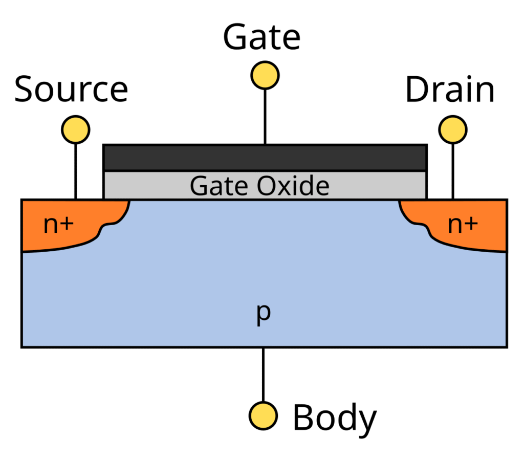
Credit: VectorVoyager (CC BY-SA 3.0)
An insulator is a type of material with electrons subjected to tight bounds, thus they do not readily lend themselves to let electrical current flow, whether it is a stream of electrons or ions – you may want to refer to S1 Section 8.a on electric current if you need more information as to its nature. At the other end, a conductor, typically a metal, is a material with weaker electron bounds, thus allowing for the flowing of electric current, whether it is charged particles or electron holes. In between is what we term semi-conductors such as silicon or germanium (both in group 14 of the Periodic table of the Elements – refer to S1 Section 2.c) with some degree of conductivity that can be engineered to exhibit different properties such as variable resistance or an asymmetrical degree of friendliness with regards to electric current directionality. Specifically, by adding some chemical elements to the materials, a process called “doping”, the crystal lattice is altered and will behave as an electron donor or as an electron acceptor by way of electron holes. For instance, adding elements from group 15 of the periodic table such as phosphorus or arsenic yields donors, this is n-type doping whereas using elements from group 13 such as boron or gallium is termed p-type doping and results in acceptors. The way to remember this is simply to know that the “n” refers to negative and therefore relates to electrons as the majority carriers of charge whereas “p” stands for positive with holes as the majority carriers of charge. The physics behind the different behaviours have to do with the electronic band structure and the respective proximity to either the conduction band or the valance band; I am enclosing a link to the relevant Wikipedia entry should you wish to know more about this.
The magic of the transistor lies in the interface of n-type and p-type materials, or p-n junction, and explains why this device is structured as a 3-layer sandwich with 2 n-type layers enclosing 1 p-type layer (denoted as n-p-n) or the reverse (p-n-p). At a p-n junction, electrons move from n-type towards p-type (which is to say the current flows from the p-layer to the n-layer), as it would in a diode. In the case of MOSFET in Figure 1, the ability for current to flow from the source to the drain depends on the application of voltage at the gate terminal above a certain threshold, which creates a conductive channel for the charge carriers. Hence the “field effect” naming. Conversely, in designs where there is an uninterrupted band of n-layer or p-layer, the gate can also be made to close the natural channel. The physics are complex but the idea relatively simple: like the name suggests it is all about creating a gate that can be opened or closed to control the flow of electric current by applying either a negative or a positive voltage to a specific terminal.
So, we have our transistors, how do we create our NAND gate then? We need to chain two of those switches and add a device called a pull-up resistor so that if any of the switches is open, corresponding to an OFF or 0 value, then the pull up resistor delivers a high value (ON or 1) and if both switches are closed then the current short circuits to ground and delivers a low value (OFF or 0). In practice, the pull-up resistor functionality is reproduced by 2 p-type transistors. Thus, with 4 transistors (2 being n-type and 2 p-type) we have a NAND gate since the circuit only shorts to ground when both A and B are ON (high value).
d) Integrated circuits and microchip manufacturing
The need to control voltage below or above certain thresholds, chain transistors and provide other properties that may be required for computing or other type of electronics calls for different elements such as resistors, capacitors (for temporary energy storage), data storage, and wiring to link them up. Altogether, these form electronic circuits and several of them are generally required to work in tandem. To allow shrinking in terms of size, production cost and energy requirement, several manufacturing techniques have developed so that nowadays, all the components are directly etched on one single piece of semiconductor material; this integrated circuit is colloquially known as microchip.
Manufacturing of microchips is a high-precision job, quite an understatement given that the most advanced technology at the time of writing this chapter has a minimum distance between transistors’ gates of under 50nm and the separation between wirings called metal pitch is about half as much. And the gates are no longer just plates, in FinFET architecture they surround the channel on three sides and the newly adopted Gate-all-Around architecture completely surrounds it on 4 sides. These aforementioned dimensions are the ones that really matter and the 3nm node you may hear about is only marketing without any representative basis. These numbers should be put in context of the extreme UV wavelength of 13.5nm used in the manufacturing process so it seems that even though some progress can still be made in miniaturization, the next steps will be not to shrink transistors much further but to stack them, using the height dimension to better effect. And perhaps make bigger chips as well, and cool them, etc.
I mentioned extreme UV light in the above paragraph, so you may rightfully ask what has light and particular wavelength to do with chip manufacturing. The answer is: quite a lot. Applying mechanical force to engrave all the required shapes over each layer of a semiconductor device would be too imprecise and risk damaging the previous work done. Instead, the solution consists in creating a pattern on a chip and then etch, i.e. remove, the parts of the layer that are not located beneath the pattern. The etching is typically done by targeting a wafer with a plasma of reactive gases in a perfectly vertical direction to avoid undercutting the material under the pattern which acts as a shield. To clarify, a wafer is a round slice of semiconductor, the substrate being crystalline silicon, from which several microchips will ultimately be produced at one go and all this work happens in the clean room of a foundry.
To get the desired pattern, a photosensitive material is spread over the entire surface of the substrate and a photomask is then aligned so that it only lets particular areas be exposed to the extreme UV light being shone on it. In the case of a positive photoresist, this exposure chemically alters the material by breaking some bonds so it can be dissolved by a certain substance called the photoresist developer and the semiconductor layer below it can then be etched. This is the high-level idea of photolithography, literally the engraving with light; in practice there are several hundred steps required for the production of modern microchips, in part because there are sometimes dozens of layers comprising transistors and wires or “connects” for each of them, and each of these layers undergoes this type of photolithography and etching process before the semiconductor doping takes place and an insulating layer is deposited followed by another layer to be etched. Rinse and repeat. Thus, the entire production process for one wafer can take up to 3 months.
e) Computing efficiency
Ultimately, the computing power of a computer is determined by three factors: #1 the speed at which operations are carried out, which is a direct consequence of how fast the electrical signal can travel through the circuits and transistors without creating any error, #2 how many computing agents are contained in the microchip, and #3 the ability to carry out several computing tasks in parallel to maximize the microchip capabilities and also avoid some execution threads being held up for too long while waiting for the current process to be completed.
The first factor is directly tied to the clock speed, or clock rate, of the microprocessor expressed as a frequency in Hertz, or should I write in GHz nowadays. The clock speed is determined by an electronic oscillator producing an analog sine wave that is translated into a digital signal conveyed across the microchip such that all signals are delivered in line with the central clock pulse. The maximum frequency of operation is limited by the heat being created then dissipated and the time taken by the electronic signal to transition between 0 and 1 states, or the opposite.
The second is the other brute force aspect: shrink transistor size to pack more in a smaller surface and therefore put more processing units on a single microchip. We call these multi-core processors.
With several cores, it becomes easy to partially address the parallel processing issue as they conveniently allow for the carrying out of multiple execution threads, a property appropriately termed multithreading. This parallel processing across various cores can also be realized within a single core if designed to do so. Essentially the idea is to split a single core into several virtual ones but of course this requires a specific architecture. Intel’s proprietary name for this capability is hyper-threading.
Processing architectures designed to run a large number of workloads in parallel has existed for a while but not so much in CPUs, the central processing units of our consumer computers. Instead, they have been a key feature of graphic processing units (GPUs), because the rendering of graphics involves computations with little dependency, meaning they can easily be run independently of each other. Hence, GPUs are designed as a cluster of hundreds or even thousands of cores. Somewhat unexpectedly, this property became very much sought after with the rise of large language models because the training of neural networks involves a lot of computations across huge datasets and a lot of these can be tackled simultaneously.
f) Trivia – Quantum computing
And so we have progressed towards ever more powerful computing devices, pushing the limits of what a transistor, or should we say a digital-based information processing can accomplish. We can still expect incremental improvements, with further miniaturization, more cores, more efficient microchips or higher clock rates and smarter architectures but beyond this “classical” computing lurks a potential revolution named “quantum” computing.
You may want to refresh your mind about quantum mechanics by (re)reading S1 Section 9.b or hopefully you recall about wave-particle duality with the wave function effectively reflecting a probability distribution. The idea behind quantum computing is that a bit of data is not either 0 or 1, as is the case in digital computing, and instead quantum bits have probabilities of being worth 0 or 1 when measured; what is termed a superposition state. The sum of these probabilities for all possible values is of course equal to 1 (i.e. 100%), as they are for classical digital bits, but the distribution is not concentrated on points 0 and 1. Rather, the probability distribution occupies an entire surface, effectively that of a 2-sphere – this should be reminiscent of the discussions about the geometry of the universe we went through in S3 Section 7.c.
A quantum bit is colloquially called “qubit” and noted “ψ”, pronounced psi. Its state is formulated as |ψ⟩ = α|0⟩+β|1⟩ where α and β are complex numbers representing the probability amplitude with the condition of the sum of their absolute square (also called squared modulus) being equal to 1: |α|2 + |β|2 = 1.
I am including a link for the Wikipedia entry on Qubit if you want to understand this better, it includes a Bloch sphere diagram.
The attraction of the qubit is that it represents a two-dimensional vector and when operating in tandem with a second qubit, the dimension of the state space is doubled, or in layman terms, twice as many values can be tested in parallel. In a n-qubit system, the number becomes 2n-dimensional, thus quantum computing power increases exponentially.
Now, don’t be alarmed or exuberant just yet. There are many practical issues to be solved including errors due to decoherence or noise in the system, the challenge in setting values to variables, the reading out of possible solutions which ties in with the measurement problem of only being able to measure one value at one time, the impossibility to clone values and the difficulty in storing them.
I am still highly sceptical we have the right reasoning to explain what we call quantum mechanics so I can only be doubtful of our ability to deliver general purpose quantum computing but what has been achieved so far is admittedly very impressive.
g) Further reading (S4C1)
Suggested reads:
- Wikipedia on NAND logic: https://en.wikipedia.org/wiki/NAND_logic
- Wikipedia on Vacuum tube: https://en.wikipedia.org/wiki/Vacuum_tube
- Wikipedia on Valance and conduction bands: https://en.wikipedia.org/wiki/Valence_and_conduction_bands
- Wikipedia on Qubit: https://en.wikipedia.org/wiki/Qubit
Next Chapter: Digital Data storage